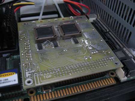
Projekt zespołowy Studenciego Koła Inżynierii Kosmicznej stanowiący część komputera pokładowego satelity SSETI ESEO. Moduł odpowiedzialny jest za stworzenie redundantnego medium komunikacyjnego wymiany danych pomiędzy podsystemami satelity poprzez magistralę CAN. Poniżej udostepniam dokumentację techniczną w języku angielskim.

DOCUMENT REVISION: 1.1.2 (26.03.2007)
Introduction
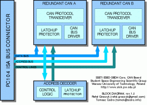
CAN BOARD is a subsystem of On-Board-Data-Handling system (OBDH Core) on SSETI ESEO satellite. It uses PC104 standard 8-bit ISA bus to exchange information with computer and two Intel’s AN82527 transceivers to exchange information on CAN network. CAN bus driving is done by Philip’s PCA82C250. Design provides simple latchup detection and protection mechanism – there are circuits onboard that measure current and can act as circuit breakers when needed.
 CANBRD Subsystem Block Diagram
ISA BUS is used to exchange information between computer and CAN transceivers. Sending or receiving packets on CAN network is done by writing or reading from internal registers of CAN transceivers. Such transceiver is a physical integrated circuit mounted on PCB and it has registers numbered from 00h to FFh that can be logicaly accessed by compuyer via ISA BUS.
CAN BOARD
CANBRD Subsystem is connected to computer via PC104 standard ISA BUS and uses 8-bit transfer mode to exchange information. In this mode data are transferred to/from SD0..SD7 lines (data bus), addres is taken from SA0..SA17 lines (data address bus). ISA BUS provides 5V power supply to subsystem (Vcc, GND) and master RESET signal. Because isa-reset is active high and CAN transceivers use active-low reset, this signal is iverted by IC5A.
Both CAN Transceivers and Latchup Protectors can generate active-low-level IRQ to the computer to inform about programmed events and minimalise bus load. IRQ can be selected by jumpres – one for latchup and two for CAN BUS. Outputs generating interrupts are open drain type.
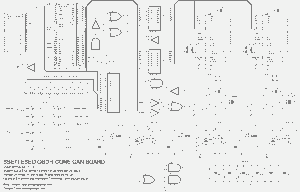
 CANBRD Subsystem Electrical Schematic
Address space
CANBRD Subsystem uses I/O address space and #IOR, #IOW control lines to select read/write operation. #IOW low starts write operation, #IOR low starts read operation. Because these lines can also be used during DMA transfers (that should not affect our subsystem) additionaly AEN line is use d to sense proper IO operation. This is why AEN line is connected do addres decoder.
Another signal used in addressing is BALE – it latches data address into transceivers and address latch onboard (IC2).
Address decoder
As there are two CAN transmitters onboard, each one has its own registers, address decoding must take place. Computer uses addressing to tell where to look for data. Addres decoder is circuit that activates first or second chip when both one of its addresses is set on the address bus, and operation is an IO type (#IOR/#IOW active). High addresses portion bits (A10..A17) can be defined manually by J9..J16 pins. Bits A0..A7 selects number of internal register to read/write to. Bits A8 and A9 are responsible for selecting first (A8,A9=11) or second (A8,A9=00 or 10 or 01) CAN transceiver chip by the address decoder.
Why it is not only one bit to select first or second chip? Both A8 and A9 bits are pulled high. When one of these bits gets damaged there is a chance that it will be in high state, then it is still possible to set other bit low and select other chip, as low logical level is “stronger” than high pullup. When there was only one bit, there would be no chance to do that.
Address decoder in details
AEN line enables comparator output (IC3) that verifies higher address space. If bits A10..A17 on addres bus are equal to those set by jumpers, P=Q output gets (active) low. This means that current address is targeted to our subsystem and it is I/O isa bus cycle (ALE=low).
This signal is gated OR (IC6B and IC6D) with AND(A8,A9). When A8 and A9 are set high, output of IC6B gets low selecting second CAN transceiver to use (#ChipEnable2 is active low signal). When A8 or A9 is set low, IC6D output gets low selecting first CAN transceiver to use (#CE1=low). When output of the higher address portion comparator (IC3) is inactive (high) because of AEN=high or address mismatch, both #CE1 and #CE2 are set hight disabling CAN transceivers.
It is important to react only on IO operations on the bus, not to interfere with MEMR/MEMW memory access. IC5B and IC5E plus IC6C monitors #IOR and #IOW lines on the ISA Bus. When an IO operation takes place, IC6C output goes high disabling address latch (IC2) output and let data show up on the internal bus (AD0..AD7). Both IC6C output signal (IO operation) along with #CE signal (correct addres on the bus), via IC7B and-gate, have influence on the bus driver IC1. IC1 is responsible to transmit data or read data from ISA Bus only when needed.
CAN Transceivers, internal multiplexed bus
Communication on CAN network is done by CAN protocol driver, Intel’s AN82527 and CAN BUS driver, Philip’s PCA82C250. Because AN82527 works in mode 0, multiplexed 8-bit intel mode, there is need to use address latch (IC2) and data direction buffer (IC1). Multiplexing in this case means using the same bus for data and addresses transfers.
Multiplexed data and address bus in details
ISA BUS control signal BALE, latches addresses into IC2 and CAN transceviers. When BALE is high IC2 is transparent – ISA address bus signals A0..A7 are passed to AD0..AD7. When BALE becomes low, AD0..AD7 becomes latched and immune to changes on A0..A7.
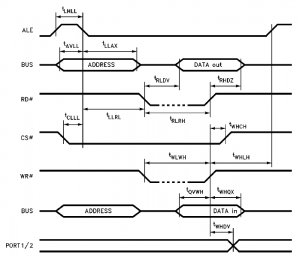
 Example AN82527 Dataflow
Because bus is being used for addressing and data transfers, simple circuity must control dataflow.
When #IOW or #IOR becomes low, this means end of addresing phase and start of data read/write phase. Then, address latch (IC2) must be disabled by turning its output into high impedance state to allow data flow on the bus. But also data buffer (IC1) must be enabled (G signal low) to pass data from/to ISA bus and CAN transceiver. Dataflow direction of this buffer is selected by DIR pin that is connected directly to #IOR ISA bus signal – when #IOR=DIR becomes low data are passed from B port to A port – this is exactly what we need to read data. When #IOR=DIR becomes high, that means write cycle, data are passed from A port to B port.
Latch IC2 is enabled when OC=0, when OC=1 outputs are in high impedance state. Data buffer is enabled when G=0, when G=1 outputs are in high impedance state. A high impedance state means that other data can flow on the bus undharmed by outputs that are in high impedance state.
Latchup protection
There are three independent latchup protection circuits onboard – two for each one of CAN blocks and one for address decoder. Single protection circuit is made of circuit breaker that is connected serially between protected circuit and power supply. In case of SEL/SEU event, current increases drasticaly – this is detected by current limiter and power is turned off.
Latchup protection in details
The LTC1153 electronic circuit breaker (IC13, IC14, IC15) drives a N-channel MOSFET (T1, T2, T3) to interrupt power to a sensitive electronic load in the event of an over-current condition. Over-current condition have place when voltage between Vs and DS pins exceeds 100mV. There are three 1ohm resistors connected parallely to gain 1/3ohm resistance, that gives about 300mA current limit to the protected circuits. There are also three resistors (0.25W each, 1206 package ) to avoid overcurrent condition burn this path of power supply.
The breaker remains tripped for a period of time set by an external timing capacitor (Ct pin) and then is automatically reset. This cycle continues until the over-current condition is removed, protecting both the sensitive load and the MOSFET switch.
An open-drain output (status pin of each protector) is provided to report breaker status to the computer by an IRQ. IRQ can be selected by jumpers.
Rafał Graczyk, Tomasz Cedro, Student Space Engineering Scientific Group, Warsaw University of Technology, Poland